July 2024
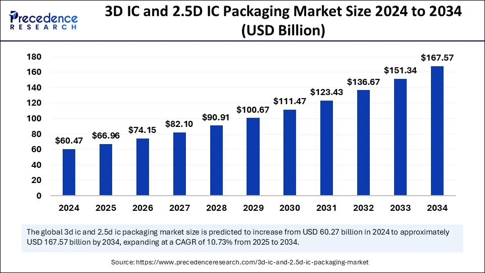
The global 3D IC and 2.5D IC packaging market size is calculated at USD 66.96 billion in 2025 and is forecasted to reach around USD 167.57 billion by 2034, accelerating at a CAGR of 10.73% from 2025 to 2034. The market sizing and forecasts are revenue-based (USD Million/Billion), with 2024 as the base year.
The global 3D IC and 2.5D IC packaging market size accounted for USD 60.47 billion in 2024 and is predicted to increase from USD 66.96 billion in 2025 to approximately USD 167.57 billion by 2034, expanding at a CAGR of 10.73% from 2025 to 2034. The increasing production of compact and high-performance electronic devices is expected to boost the growth of the market during the forecast period.

Artificial intelligence (AI) plays a significant role in the development of 3D IC and 2.5D IC packaging. AI technology helps in identifying new materials, which can help enhance the quality, reliability, and performance of these IC packaging solutions. AI and machine learning (ML) algorithms can help accelerate the research and development processes. These algorithms analyze huge amounts of data to find materials or compositions that suit specific applications. It helps in evaluating novel materials through data analysis for enhanced packaging solutions. AI-based systems can assist in manufacturing, improving production output. AI also automates tedious tasks and reduces errors, ensuring that the packaging meets stringent quality standards. With AI's predictive maintenance capabilities, it is possible to identify flaws in manufacturing processes and avoid sudden disruptions. AI tools can help maintain consistent quality as any defect is quickly identified in real time. AI technology helps optimize operations, accelerate R&D activities, enhance efficiency, and maintain quality, further boosting this market’s growth.
The 3D IC packaging consists of the integration of multiple layers or vertical stacking of dies, which helps create a three-dimensional structure. On the other hand, the 2.5D IC packaging is the integration of multiple chips or dies with a silicon interposer or organic substrate. Ongoing advancements in semiconductor packaging technologies are one of the key factors boosting the growth of the 3D IC and 2.5D IC packaging market. These packaging solutions are easy to integrate into the complex and smaller architecture of the electronics devices. There is a rising demand for consumer electronics, which is boosting the growth of this market. In addition, the rising government initiatives to boost the production of semiconductors directly impact this market's growth.
| Report Coverage | Details |
| Market Size by 2034 | USD 167.57 Billion |
| Market Size in 2025 | USD 66.96 Billion |
| Market Size in 2024 | USD 60.47 Billion |
| Market Growth Rate from 2025 to 2034 | CAGR of 10.73% |
| Dominated Region | Asia Pacific |
| Fastest Growing Market | North America |
| Base Year | 2024 |
| Forecast Period | 2025 to 2034 |
| Segments Covered | Packaging Technology, Applications, End Use, and Regions. |
| Regions Covered | North America, Europe, Asia-Pacific, Latin America and Middle East & Africa |
Growing Demand for High-Performance Consumer Electronics
The rising demand for high-performance consumer electronics is a key factor driving the growth of the 3D IC and 2.5D IC packaging market. 3D IC and 2.5 D IC packaging enable the stacking of multiple semiconductor chips, improving processing power and memory bandwidth. This further enhances the overall performance of electronic devices. With the rising penetration of internet services all over the world, the adoption of consumer electronics such as smartphones, tablets, gaming consoles, wearables, and laptops is increasing rapidly. For instance, in the third quarter of 2024, smartphone shipments reached 46 million units, with 5.6% year-over-year growth in India alone. As the production and adoption of consumer electronics rise, so does the need for semiconductors, which significantly boosts the demand for 3D IC and 2.5 IC packaging. In addition, the growing trend of miniaturization in electronic devices drives market growth. As electronic devices become more compact, the 3D IC and 2.5D IC packaging emerge as an ideal solution to improve devices’ performance and efficiency.
Technical Challenges
The technical challenges involved in manufacturing processes are the major factors limiting the growth of the 3D IC and 2.5D IC packaging market. 3D IC and 2.5D IC packaging techniques are used to combine various chips into one pack. However, combining different technologies into one package creates heat dissipation and power management challenges. Moreover, ensuring the compatibility and reliability of these packaging is challenging. The manufacturing processes of these packaging are complex, requiring specialized equipment. This, in turn, increases the production costs, limiting the market growth.
Focus on Sustainability
Stringent regulations regarding environmental sustainability are encouraging electronic device manufacturers to focus on sustainable practices. This, in turn, boosts the demand for 3D IC and 2.5 IC packaging. This packaging led to the development of power-efficient devices, reducing energy consumption and carbon emissions. Moreover, 3D IC and 2.5 IC packaging increase the lifespan of consumer electronics by reducing the replacement of semiconductor chips and overall weight. With the rising production of compact electronics, the need for smaller packaging sizes is increasing, creating lucrative opportunities in the market.
The 3D wafer-level chip-scale packaging (WLCSP) segment dominated the 3D IC and 2.5D IC packaging market in 2024. The segment growth is mainly driven by the rise in the production of compact electronic devices. This packaging technology offers compact packaging, reducing the overall weight of electronic devices. There is a necessity for packaging solutions for smaller and lighter components in modern electronic devices. This packaging allows the integration of advanced cooling solutions, which is effective in densely packed circuits. Such aspects make this packaging a popular choice.
The 3D through-silicon via (TSV) segment is projected to grow at the fastest rate in the coming years. 3D TSV packaging technology is used to connect multiple semiconductor dies. This technology is suitable for smaller, faster, and more power-efficient devices. The rising demand for high-performance electronic devices is expected to drive segmental growth.
The MEMS/Sensors segment led the 3D IC and 2.5D IC packaging market with the largest share in 2024. This is mainly due to the rising miniaturization of electronic devices, which boosts the demand for micro-electro-mechanical systems (MEMS). 3D IC and 2.5D IC packaging are essential for MEMS and sensors. With multiple vertical die stacking or blending of different components in one package, the MEMS size can be reduced without affecting the performance. It also helps sensors to be properly integrated into different applications in minimum space like in medical devices, automobiles, and wearables.
The imaging & optoelectronics segment is expected to grow at a rapid pace during the forecast period. The 3D IC and 2.5D IC packaging enable the integration of multiple sensors in a compact space, improving the performance of imaging systems and optoelectronics. This packaging enables the development of more compact imaging and optical devices. The rising demand for imaging systems and optoelectronic devices in various industries supports segmental growth.
The consumer electronics segment dominated the 3D IC and 2.5D IC packaging market in 2024. The growth of the segment is mainly driven by the increasing demand for consumer electronics across the world. The rise in the necessity of memory requirements in electronics like smartphones has boosted the demand for advanced memory technology integration. As the production and demand for consumer electronics increases, so does the need for 3D IC and 2.5D IC packaging to stack multiple semiconductors die. The rising demand for high-performance compact electronic devices further sustain the segment’s position.
Asia Pacific held the largest share of the 3D IC and 2.5D IC packaging market in 2024. The regional market growth is driven by the strong presence of the semiconductor manufacturing industry, boosting the demand for advanced packaging solutions. The region is home to some of the leading electronics, automotive, and medical device manufacturing companies, boosting the demand for semiconductors. Governments around the region are also investing heavily to boost the domestic production of semiconductors. A significant rise in the production of consumer electronics further bolstered the market growth in the region.
Countries like China, Japan, India, Taiwan, and South Korea play a crucial in the Asia Pacific 3D IC and 2.5D IC packaging market. Taiwan is the world’s largest producer of semiconductors, followed by South Korea and China. In addition, China is a major hub for electronic device manufacturing, boosting the demand for semiconductor chips, and so does the need for advanced packaging technologies. Moreover, the rising production of smart electronics and automotive components contributes to market growth.
North America is poised to witness the fastest growth during the forecast period. The region boasts leading automotive, semiconductor, aerospace, and medical device companies, which is a key factor boosting the growth of the market in the region. There is a high demand for smart and cutting-edge consumer electronics, like smartphones, tablets, and laptops, in which advanced packaging technologies, including 3D IC and 2.5D IC packaging, play a crucial role in improving performance and efficiency. In addition, the rising adoption of advanced technologies like AI-driven systems and Internet of Things (IoT) devices contributes to regional market growth.
The U.S. is expected to have a stronghold on the North American 3D IC and 2.5D IC packaging market. The country is home to leading semiconductor companies such as NVIDIA and Intel, providing a strong foundation for advancing IC packaging technologies. There is a high demand for high-end consumer electronics, such as wearables and smart appliances, which rely on semiconductor chips. Moreover, the increasing demand for high-performance computing and data centers boosts market growth.
Europe is projected to show notable growth during the forecast period. The rising government initiatives to boost domestic semiconductor production support regional market growth. For instance, the European Union has implemented the European Chips Act to boost semiconductor production and reduce reliance on external suppliers. Under this Act, the region aims to increase its share of global semiconductor production to 20% by 2030. In addition, the rising adoption of advanced technologies, increasing demand for smart consumer electronics, and the presence of well-known automakers that are focusing on boosting the production of EVs are expected to drive market growth in the region.

By Packaging Technology
By Application
By End Use
By Region
For inquiries regarding discounts, bulk purchases, or customization requests, please contact us at sales@precedenceresearch.com
No cookie-cutter, only authentic analysis – take the 1st step to become a Precedence Research client
July 2024
February 2025
July 2024
August 2024