July 2024
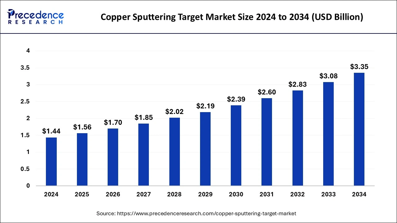
The global copper sputtering target market size is calculated at USD 1.56 billion in 2025 and is forecasted to reach around USD 3.35 billion by 2034, accelerating at a CAGR of 7.83% from 2025 to 2034. The North America copper sputtering target market size surpassed USD 600 million in 2024 and is expanding at a CAGR of 9% during the forecast period. The market sizing and forecasts are revenue-based (USD Million/Billion), with 2024 as the base year.
The global copper sputtering target market size was estimated at USD 1.44 billion in 2024 and is anticipated to reach around USD 3.35 billion by 2034, expanding at a CAGR of 7.83% from 2025 to 2034.

AI is significantly impacting the copper industry across various operational facets. Integration of AI in copper sputtering enhances efficiency and safety along with environmental compliance. AI algorithms detect trends in major copper using sectors like semiconductor industry, construction and electronics industry. This allows the producer to foresee demand for the copper and its market value which further affects the production schedules proactively.
Such strategic approach about deployment of AI fix that, the copper industry can meet the global demand effectively while ensuring sustainability by avoiding unnecessary production and utilization of resources.
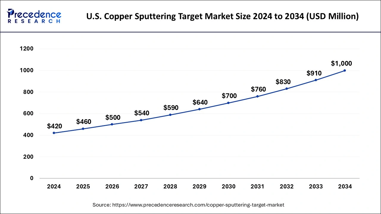
The U.S. copper sputtering target market size was evaluated at USD 420 million in 2024 and is predicted to be worth around USD 1000 million by 2034, rising at a CAGR of 9.06% from 2025 to 2034.

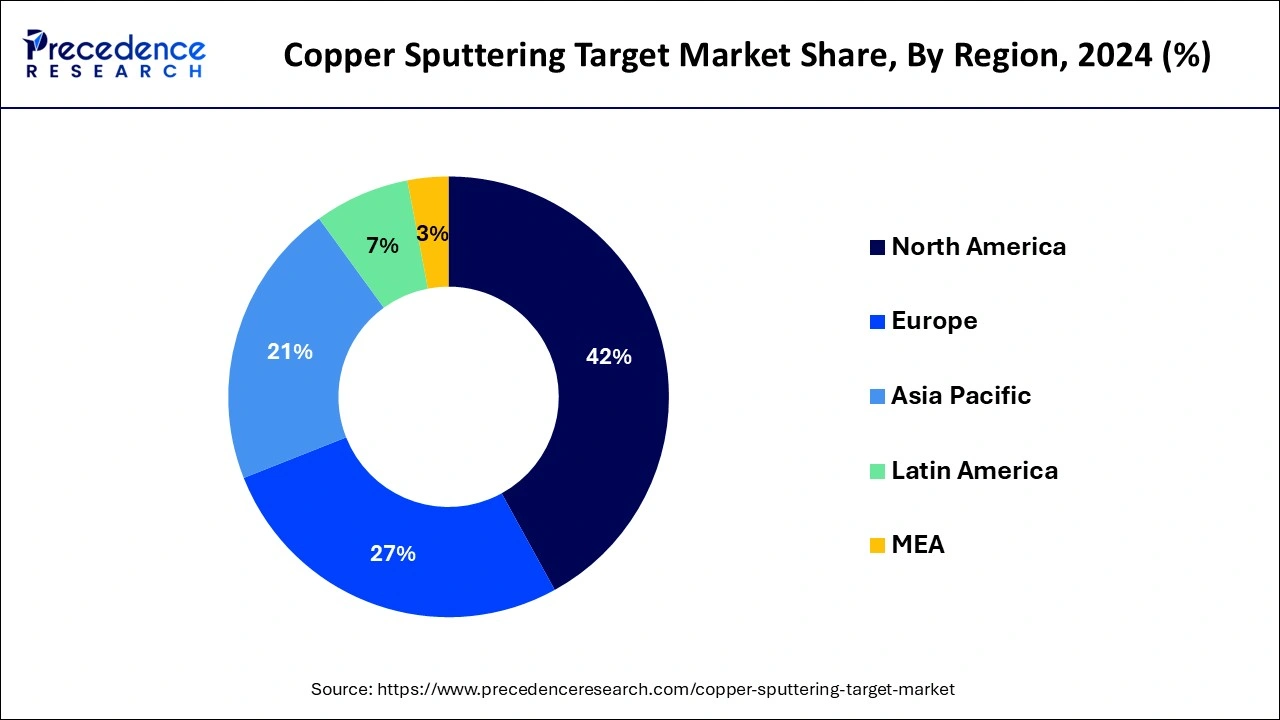
Given the rising demand for semiconductors, solar cells, and LCDs, dominated the global copper sputtering target market with the largest market share of 42% in 2024.

The market is expanding in Europe as a result of rising demand for high-purity items such as copper sputtering targets with ultra-high purity. Due to the rising demand for copper sputtering targets across a range of industries, including semiconductors, LCDs, solar cells, and others, the Asia Pacific is anticipated to experience considerable expansion over the course of the projected period.
Sputtering targets are materials that are subjected to physical vapor deposition (PVD), a process that involves the high-velocity ejection of atoms from solids. The atoms that are ejected after depositing on the workpiece produce a thin film coating with beneficial properties. There is a transfer of momentum that occurs when high-energy ions collide with the atoms of the target substance. Multiple collisions can occur at times. Due to long-distance flight, the ions occasionally lose energy. If the energy of the ions travelling to the target is higher than the energy of the bonds holding the atoms of the target material together, the colliding atoms will detach from the target material, a process known as sputtering. And the production of thin coatings on the target that range in thickness from a few nanometers to a few micrometres occurs during copper sputtering, a sort of deposition technique.
Gaseous atoms are released when the target materials split apart. These thermodynamically unstable atoms often live on a surface in a vacuum. The thin film is a coating of atoms that is formed on the target and is a micrometre thick. Using copper sputtering targets, the semiconductor and solar industries manufacture solar cells and other electrical devices. Using the sputtering method, a thin layer of an ultra-pure metallic or oxide substance can be deposited on another solid material. A component capable of high-speed computer operation is now being developed using copper sputtering targets with low electric resistance. The copper sputtering target’s normal grain size is around 30 m, and 17% of the heterogeneities are formed by annealing at a temperature of 0.4 Tm in order to achieve uniformity in the thin layer that is created. Gases including krypton, xenon, neon, and argon are used in the copper sputtering procedure. Copper sputtering targets can be set up from projects in research and development to production teams, covering medium to large substrate regions, for effective energy directed to the target mass.
| Report Coverage | Details |
| Market Size in 2025 | USD 1.56 Billion |
| Market Size By 2034 | USD 3.35 Billion |
| Growth Rate from 2025 to 2034 | CAGR of 7.83% |
| Base Year |
2024 |
| Forecast Period |
2025 to 2034 |
| Largest Market | North America |
| Segments Covered | Product, Application |
| Regions Covered | North America, Europe, Asia-Pacific, Latin America, and Middle East & Africa |
Increased use of copper as a sputtering target for semiconductor chips will fuel industry expansion.
The use of copper-sputtering targets for semiconductor devices is predicted to rise during the time of the projection, fueling expansion in the global market for copper-sputtering targets. The sputtering target is used to create the barrier layer and the packaging metal wiring layer. The metal grid, barrier layer, and conductive layer of the wafer are produced largely using the target material throughout the wafer manufacturing process. Using the sputtering target material, the chip packaging method produces the wiring layer, the metal layer behind the bump, and other metal parts. Despite the small number of target materials used in wafer manufacturing and chip packaging, according to SEMI figures, their cost accounts for around 3% of the total cost of the wafer manufacturing and packaging process. Sputtering target materials are one of the primary raw materials used in the production of semiconductors because they directly affect the uniformity and performance of the conductive layer and barrier layer as well as chip transmission speed and stability.
The market's growth is hampered by the challenge of uniformly setting targets for complicated structures.
Two of the major obstacles for the worldwide copper sputtering business are the inability to reliably place targets with complex geometries and the sluggish deposition rate for specific materials in the sputtering target technology. The technological advancements and innovations produced by both established and upcoming producers in the copper-sputtering target market are also expected to hasten the resolution of these issues.
Consumer electronics semiconductor advancements offer a significant prospect for market expansion.
The development of semiconductors for consumer devices like smartphones, tablets, and laptops is likely to assist the growth of the global copper-sputtering target market during the forecasted period. For instance, IBM introduced strides in the design and manufacturing of semiconductors in May 2021 when it unveiled the first chip in the world to use 2 nm Nano sheet technology. Almost every area of modern life uses semiconductors, including computing, appliances, communications, transportation, and essential infrastructure. Improved chip performance and energy efficiency are in high demand, especially in the era of hybrid clouds, AI, and the Internet of Things. IBM has created cutting-edge 2-nanometer chip technology to help the semiconductor industry keep up with this growing demand. It is projected to perform 45% better or consume 75% less energy than the most recent 7 nm node products. As a result, these improvements in the business offer a lucrative opportunity for market expansion.
Based on techniques copper sputtering is divided into copper sputtering with low purity, copper sputtering with high purity, and ultra-high-copper sputtering.
This market is divided into Solar cells, LCD displays, semiconductors, Solar Cells, LCD Displays and others.

By Technique
By Application
By Geography
For inquiries regarding discounts, bulk purchases, or customization requests, please contact us at sales@precedenceresearch.com
No cookie-cutter, only authentic analysis – take the 1st step to become a Precedence Research client
July 2024